SEMITOP® Benefits
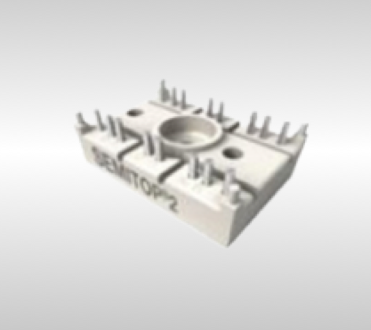
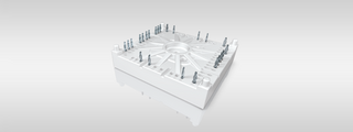
The SEMITOP platform centres around 12-mm-high modules, covering the low and medium power range, with one or two mounting screws and no baseplate. The PCB interface can be made via solder or press-fit pins. The low commutation inductance design and the choice of the latest Si and SiC chip technologies make this product suitable for UPS, solar, energy storage, motor drives, power supplies, welding and EV charger markets. A large variety of configurations are possible within the SEMITOP family, including 3-level (NPC/TNPC) and CIB (converter-inverter-brake) topologies.
SEMITOP® Product Family
- SEMITOP® Classic
Complete 12mm module-family with PCB connection via solder or press-fit pins. Low commutation inductance design and the availability of latest Si and SiC chip technologies bring maximum performance in its class.
- SEMITOP® E1/E2

SEMITOP E1 and E2 were developed to offer an alternative to the consolidated standard industrial packages in order to ensure supply chain safety at high levels of performance.
SEMITOP® Short Facts
- 12mm module height
- Reliable solder or press-fit connection
- Low stray inductance case
- Optimized thermal performance
SEMITOP® Key Features
- Baseplate-less design
- Press-fit or solder terminals
- Complex configurations possible
- Different chip technologies and manufacturers available
- Optimized system costs
SEMITOP® Applications
The SEMITOP family features a cost-effective design. This product generation is designed for the low and medium power range of up to 200kW following the latest introduction of the SEMITOP E family. Compact and low inductance design, coupled with the latest chip technologies and different topologies, makes the two platforms suitable for different markets such as UPS, solar, energy storage, motor drives, power supplies and EV charger markets.
SEMITOP® Product Range
The SEMITOP portfolio includes fast Si diodes, fast 650V/1200V IGBTs and MOSFETs for high voltage. The latest SiC chip technologies for diodes and MOSFETs can be integrated in the platform, making a lot of different configurations with different chip combinations possible:
- Neutral point clamp 3-level configuration (NPC)
- T-type NPC 3-level configuration (TNPC)
- 3-phase inverter (Sixpack)
- CIB configurations (converter-inverter-brake)
- 3-phase bridge rectifier
- Full and Hybrid SiC configurations
- Customized configurations possible